It has long been recognized that confinement and reduced dimensionality constitute powerful ways of tuning the relative strength of fluctuations. Moreover, powerful methods exist in low-dimensional systems to address the many-body problem which can be brought to bear when tackling the physics of nanostructures and interfaces.
Nanostructured devices have been attracting interest of physicists and engineers alike for exploring and utilizing effects at the nanoscale and the intermediate scale between the realms of classical and quantum physics. Broadly speaking, the typical extend of a nanostructured system becomes comparable to or even smaller than characteristic scales like the phase coherence length of electrons and their mean free path, or Fermi wavelength. As a result, the classical equation of motions and thermodynamics have to be replaced by quantum mechanics and quantum statistics.
Interfaces are ubiquitous in materials science. Many modern tools to probe many-body systems are e.g. surface sensitive. Typical examples are angle-resolved photoemission spectroscopy and scanning tunneling spectroscopy. This means that these methods predominantly probe the properties of the material-vacuum or material-air interface. Another common example concerns phase separation that accompanies first order phase transitions. Interfaces are characterized by a symmetry reduction with respect to the bulk and a change in the chemical environment.
Inversion symmetry breaking at the surface can lead to Rashba splitting. The interface-derived changes to ligand fields can induce ”secondary” effects like the sp3 dehybridization and reconstruction phenomena for polar systems. These phenomena seem to be particularly relevant to oxide heterostrucures. Of particular interest to us are interfaces between superconductors and magnets and hybrid structures formed from such materials.
Highlights
“Predicting the conductance of strongly correlated molecules: the Kondo effect in perchlorotriphenylmethyl/Au junctions”
W. H. Appelt, A. Droghetti, L. Chioncel, M. M. Radonjic, E. Muñoz, S. Kirchner, D. Vollhardt, and I. Rungger
Nanoscale 10, 17738 (2018)
Stable organic radicals integrated into molecular junctions represent a practical realization of the single- orbital Anderson impurity model. Motivated by recent experiments for perchlorotriphenylmethyl (PTM) molecules contacted to gold electrodes, we develop a method that combines density functional theory (DFT), quantum transport theory, numerical renormalization group (NRG) calculations and renormalized super-perturbation theory (rSPT) to compute both equilibrium and non-equilibrium properties of strongly correlated nanoscale systems at low temperatures effectively from first principles. We determine the possible atomic structures of the interfaces between the molecule and the electrodes, which allow us to estimate the Kondo temperature and the characteristic transport properties, which compare well with experiments. By using the non-equilibrium rSPT results we assess the range of validity of equilibrium DFT + NRG-based transmission calculations for the evaluation of the finite voltage conductance. The results demonstrate that our method can provide qualitative insights into the properties of molecular junctions when the molecule–metal contacts are amorphous or generally ill-defined, and that it can further give a fully quantitative description when the experimental contact structures are well characterized.
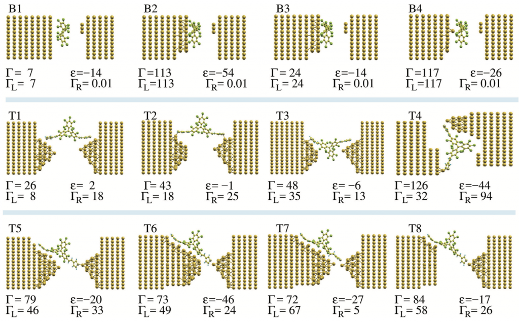
Junction geometries for bare-PTM on an Au surface (B1–B4), and for PTM-BT between two Au electrodes (T1–T8), investigated in this paper. For each junction we specify the broadening of the singly occupied molecular orbital induced by the coupling to the electrodes (Γ), its position with respect to EF (ε), and the coupling to the left and right electrodes (ΓL and ΓR, respectively; Γ = ΓL + ΓR). All units of the specified quantities are meV.
“Impact of atomic-scale contact geometry on Andreev reflection”
J. Brand, P. Ribeiro, N. Néel, S. Kirchner and J. Kröger
Phys. Rev. Lett. 118, 107001 (2017)
Charge transport has been examined in junctions comprising the normal-metal tip of a low-temperature scanning tunneling microscope, the surface of a conventional superconductor, and adsorbed C60 molecules. The Bardeen-Cooper-Schrieffer energy gap gradually evolves into a zero-bias peak with decreasing electrode separation. The peak is assigned to the spectroscopic signature of Andreev reflection. The conductance due to Andreev reflection is determined by the atomic termination of the tip apex and the molecular adsorption orientation. Transport calculations unveil the finite temperature and the strong molecule-electrode hybridization as the origin to the surprisingly good agreement between spectroscopic data and the Blonder-Tinkham-Klapwijk model that was conceived for macroscopic point contacts.
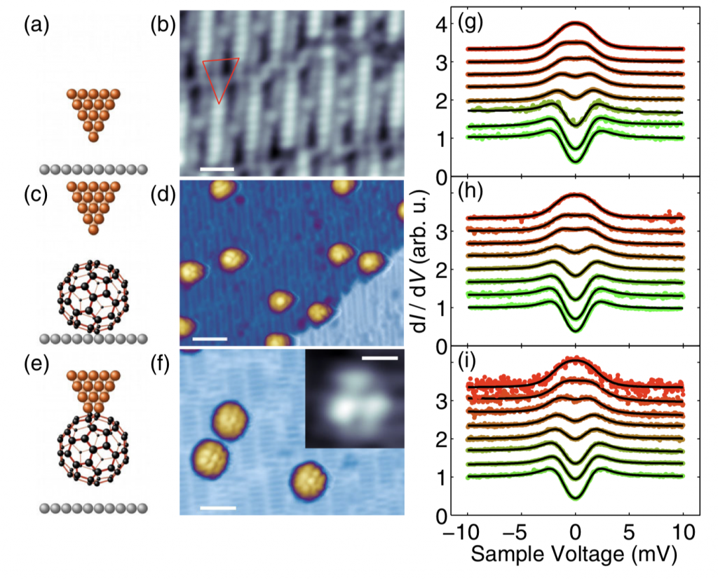
(a) Sketch of a W-Nb junction. (b) STM image of NB atom chains on NbO(111) (100 mV, 500 nA, scale bar: 1 nm). The triangle indicates the preferred C60 adsorption region. (c) Sketch of a W − C60 junction. (d) STM image of individual C60 molecules adsorbed on NbO(111) (100 mV, 50 pA, scale bar: 3 nm). C60 molecules appear as circular protrusions with submolecular structure. (e) Sketch of a C60 − Nb junction. (f) STM image of individual C60 molecules on NbO(111) acquired with a C60-terminated tip (100 mV, 50 pA, scale bar: 2 nm). Inset: STM image of an atomic protrusion on the surface revealing the C60 orientation at the tip apex (100 mV, 50 pA, scale bar: 0.5 nm). (g)–(i) Normalized dI=dV spectra (dots) of W − Nb (g), W − C60 (h), C60 − Nb (i) junctions with decreasing elec- trode separation (from bottom to top). Junction conductances range from (g) 0.20 to 1.29 G0, (h) 0.11 to 1.35 G0, (i) 0.34 to0.97 G0. Spectra are offset vertically for clarity. Full lines represent fits according to the BTK model. The color of the data sets reflects the magnitude of the BTK transmission τ (green:τ=0, red: τ=1).